July 6, 2026
CoolSem Technologies Wins the Gerard & Anton Award 2026:
Advancing the Future of Semiconductor Cooling
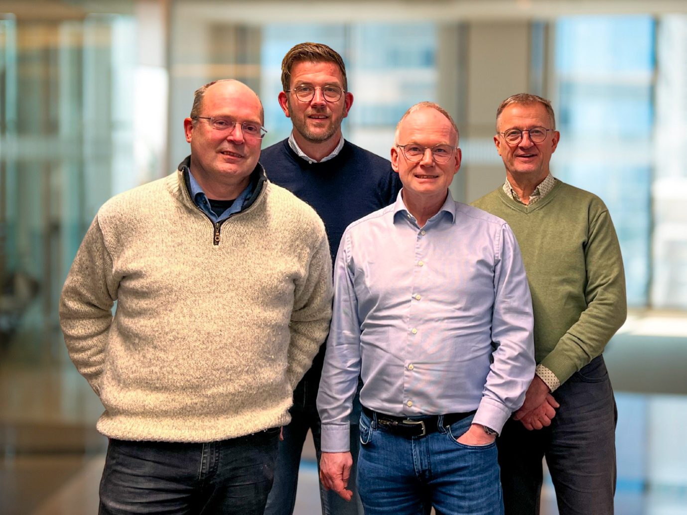
CoolSem Technologies is proud to announce that we have been awarded the Gerard & Anton Award 2026, recognizing the most promising technology startups in the Brainport Eindhoven region.
This award represents an important milestone in our journey to address one of the most fundamental challenges facing the semiconductor and photonics industries: heat.
The challenge: heat is becoming the defining constraint of next-generation semiconductors
As device performance continues to increase, thermal management is rapidly becoming a critical bottleneck affecting efficiency, reliability, lifetime, and scalability. At CoolSem Technologies, we believe that thermal management must evolve from a supporting function to a core design consideration for next-generation semiconductor and photonic devices.
Our answer to this challenge is WaLTIS® (Wafer-LevelThermal Integrated Substrate), a fundamentally new approach to thermal management that extracts heat directly from the core of semiconductor devices. By replacing conventional substrates with highly engineered multilayer thermal structures, WaLTIS® creates a significantly shorter and more efficient thermal path, enabling devices to operate cooler, more reliably, and at higher performance levels.
Tomorrow's chips will not only need to be faster, but cooler
Unlike conventional cooling solutions that address heat after it has already passed through the chip packaging layers, CoolSem tackles the problem at its source. Implemented at wafer level, WaLTIS® is designed to integrate with existing semiconductor manufacturing flows without requiring entirely new fabrication infrastructure, enabling a scalable and manufacturable route toward industrial adoption.
Hence our tagline “Cool at the Core” 😊
Cool at the Core, Serious About the Future
With a founding team that brings decades of semiconductor experience, CoolSem's technology has been designed to fit existing manufacturing flows. The process is implemented at wafer level, so the thermal stack can be applied to many devices in parallel, rather than chip by chip.
That gives WaLTIS® a credible path to scale without requiring device-by-device assembly or major redesign of the front-end device. For manufacturers, this matters: the best thermal solution is not very useful if it cannot survive the realities of semiconductor production.
Since founding CoolSem Technologies in the summer of 2025,our team has rapidly progressed from concept to technology demonstrations. The company has completed its initial proof-of-concept work and is now conducting a second technology validation cycle focused on performance, repeatability and wafer-level manufacturability.
We have assembled a highly experienced team, secured support from leading deep-tech investors and ecosystem partners, and generated strong interest from companies across the semiconductor and photonics industries.
Building Cool Technology Is a Team Sport
While we are proud of our technical achievements, one of our greatest successes has been building momentum and trust within the broader ecosystem. Deep-tech innovation is fundamentally a collaborative effort, and no success story is built alone.
We would therefore like to express our sincere gratitude to the many organizations, partners, investors, customers, and supporters who have contributed to our journey over the past year. In particular, we would like to thank the broader Brainport Eindhoven ecosystem, whose unique combination of technical expertise, entrepreneurial support, industrial networks, and patient capital has been instrumental in our development.
We are grateful for the support of organizations including PhotonDelta, Brabant Startup Fonds, Brightmove, Rabobank, and the wider Dutch semiconductor and photonics ecosystem. Their support has helped us bridge the challenging early phase between promising technology, first validation results, and industrial deployment.
This recognition motivates us even more as we continue totransform strong technical potential into industrial proof points. Our next steps include further validation of WaLTIS® at wafer level, expansion of pilot collaborations in photonics, RF, and power devices, and continued preparation for future industrial adoption.
It turns out that being "Cool at the Core" is not just our tagline. It is increasingly becoming a necessity for the future of semiconductors and photonics.
We thank everyone who has been part of our journey so fa rand look forward to the exciting next chapter ahead.
For the full report of the 2026 G&A Award winners: Gerard & Anton award winners connect tech with tangible problems
Article in IO+ Magazine on CoolSem, winner of the G&A Award 2026