Advancing chip fundamentals through material and thermal innovation.
CoolSem’s patented wafer-level thermal management technology helps chips run cooler, last longer, and perform beyond today’s limits.
CoolSem’s patented wafer-level thermal management technology helps chips run cooler, last longer, and perform beyond today’s limits.
Scroll to discover
Learn more about our mission
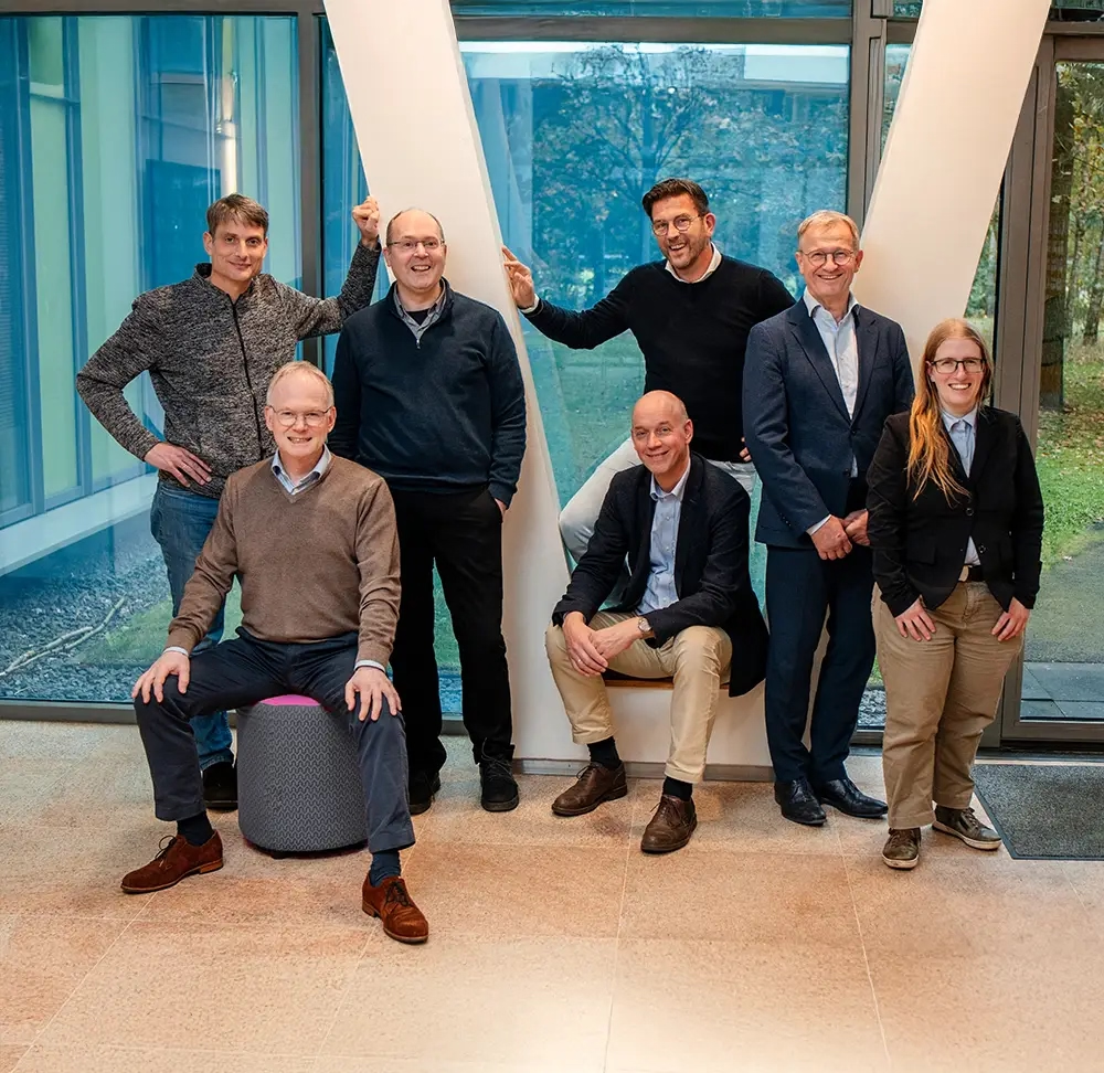

We redefine semiconductor performance through material and thermal innovation.
Watch how our team works on this mission

why heat limits chips
While traditional cooling techniques remove heat from the package or system level, the real challenge lies deeper.
In the thermal resistance of the chip’s substrate.

Active device

Substrate

heatsink
But the challenge goes deeper than heat itself.
As devices cycle through temperature changes, the different materials inside each chip expand and contract at different rates — adding mechanical stress on top of thermal resistance. Over time, this stress degrades interfaces and compounds the very heat problem it’s meant to control.

Our wafer based solution
Our wafer based solution
CoolSem removes the substrate, the barrier to efficient heat flow.
And we replace it with our patented wafer-level carrier that conducts heat up to 15× better.


Active Devices

Substrate

Waltis ®
Break the thermal bottleneck Keep the device layout
WaLTIS® replaces the original substrate with a thinner, thermally optimized wafer-level stack, reducing thermal resistance by up to 15×. This helps lower peak device temperatures and mitigate thermal hotspots, while preserving existing device layouts and electrical isolation schemes.

Key application domains
RF Base Stations
Keep RF performance high as power density rises.
5G and emerging 6G networks are driving more RF power, more channels and tighter integration into increasingly compact massive-MIMO antenna systems. At the same time, outdoor infrastructure must maintain performance and reliability across demanding temperature cycles and long service lifetimes. For high-power GaN RF devices, the substrate can become a critical thermal and thermo-mechanical bottleneck. WaLTIS replaces that substrate with a lower-resistance, CTE-matched thermal path — helping reduce junction temperature and thermal stress while supporting higher power density and long-term reliability in macro and massive-MIMO base stations.

RF & SatCom
More RF power from every antenna tile.
Next-generation satellite user terminals are moving toward thinner, electronically steered flat-panel antennas with large numbers of tightly packed RF channels. That puts increasing pressure on the power amplifiers inside each tile, where heat must be removed efficiently without adding bulk or compromising reliability. For GaAs and GaN-on-Si power amplifiers, the native substrate and device stack can limit the thermal path from the active region to the antenna baseplate. WaLTIS replaces the original substrate with a lower-resistance, CTE-matched thermal path, helping reduce junction temperatures and enabling higher power density, longer PA lifetime and more compact terminal architectures.

Photonics
Keep the light stable as density rises.
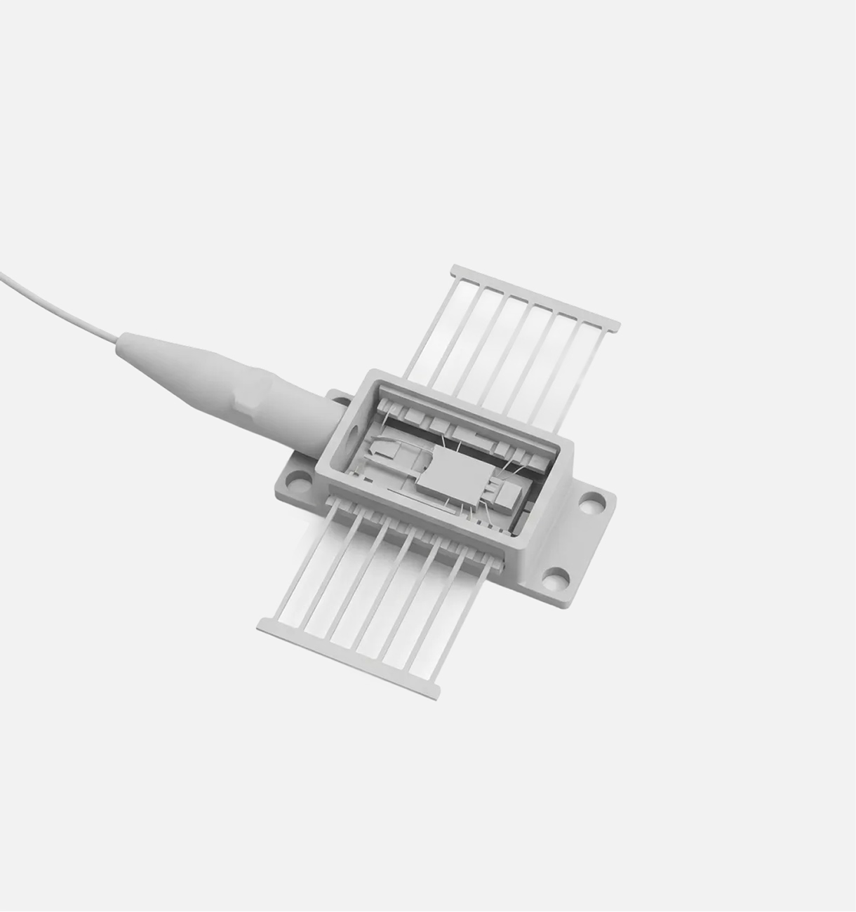
AI infrastructure is driving optical functions closer together — and closer to high-power electronics. As integration density rises, temperature stability and thermal crosstalk become increasingly critical. Lasers and integrated photonic devices are highly temperature sensitive. Localized heating can affect wavelength stability, efficiency and lifetime. WaLTIS replaces the native III-V substrate with a lower-resistance thermal path, helping reduce peak temperatures and temperature gradients across the die, enabling more stable photonic performance at higher integration density.
Power Conversion
Let wide-bandgap devices deliver their full potential.
AI data centers, electric vehicles and industrial systems are all demanding more power from less volume. SiC and GaN make that possible — but only if the thermal path can keep up. As current density and system compactness increase, the thermal path beneath the die increasingly becomes a constraint. WaLTIS tackles that bottleneck at device level, reducing thermal resistance close to the active region and helping designers translate wide-bandgap performance into higher current density, smaller systems and greater reliability.
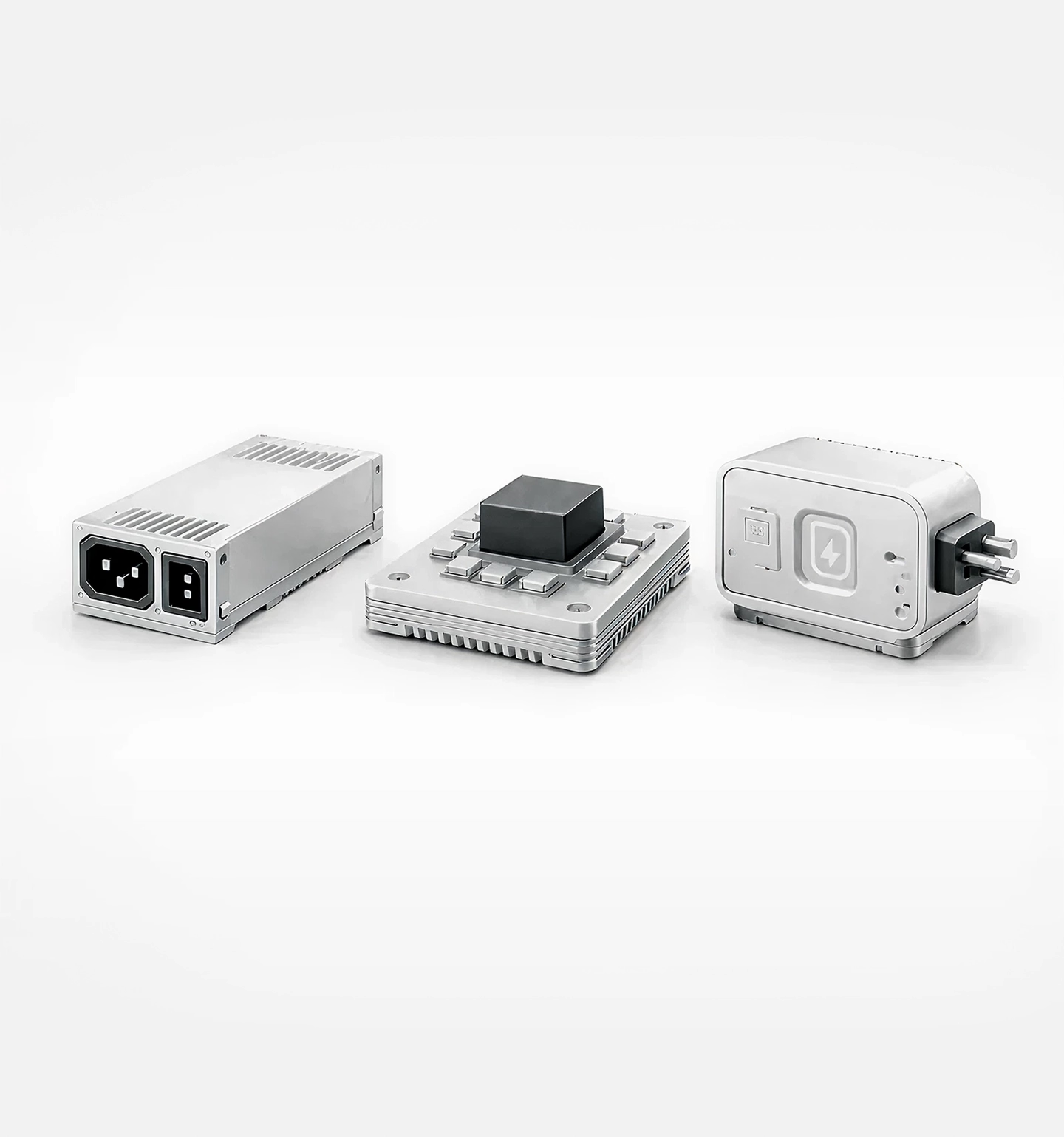



Why WaLTIS® is different
Engineered substrate for hotspot relief
WaLTIS directly targets the die-to-substrate bottleneck, lowering junction temperature and smoothing mechanical stress where GaN, GaAs, InP and SiC devices run hottest.
Front-end neutral, Back-end friendly integration
WaLTIS integrates after device fabrication, preserving existing SiC/GaN wafer lines while fitting seamlessly into today’s die-attach, DBC, and module assembly flows.
Flexible Across Platforms and Process Flows
WaLTIS integrates with varied device types and manufacturing routes, enabling high-performance substrates without altering upstream designs or downstream assembly.
What does CoolSem do?
CoolSem develops wafer-levelthermal solutions for semiconductor and photonic devices.
Our WaLTIS technology replaces the original device substrate with an engineered thermal and mechanical stack designed to improve heat removal close to the active device layer. At the same time, it can help manage coefficient of thermal expansion (CTE) mismatch between the device and the next level in the assembly.
By improving this part of the thermal path, WaLTIS can support higher performance, greater reliability, longer lifetime and more efficient system-level cooling.
What problem is CoolSem solving?
As semiconductor and photonic devices become more powerful and compact, heat and thermo-mechanical stress increasingly limit performance, reliability and integration.
High thermal resistance close to the active device can lead to higher operating temperatures, reduced efficiency, performance derating and greater demands on package- and system-level cooling. Differences in thermal expansion between materials can also create mechanical stress, particularly in larger dies, brittle semiconductor materials and applications exposed to repeated thermal cycling.
CoolSem addresses these challenges by improving the thermal and mechanical architecture at device level, close to where the heat is generated: Cool at the Core.
What is unique about CoolSem's approach?
CoolSem addresses thermal performance at device level rather than relying only on improvements further downstream in the package or cooling system.
WaLTIS replaces the original device substrate after front-end fabrication with an engineered stack, designed specifically for the thermal, mechanical and electrical requirements of the final application.
This makes it possible to improve the first part of the thermal path, where significant bottlenecks can occur, while complementing existing package- and system-level cooling solutions.
What is WaLTIS?
WaLTIS is CoolSem's Wafer-Level Thermal Interface Stack. It is an engineered wafer-level substrate consisting of multiple functional layers. WaLTIS is bonded to a thinned customer wafer and is designed to provide four main functions: improved thermal conduction from the device layer to the next level in the assembly; better CTE matching to support mechanical stability under thermal cycling; electrical isolation where required, including for high-voltage and RF applications; and mechanical support for the resulting bonded wafer stack, which is especially relevant for brittle materials such as InP. CoolSem's first generation is aimed at wafer sizes up to 200 mm, with larger wafer formats to be addressed in the second generation and through licensing models.
WaLTIS is CoolSem's Wafer-Level Thermal Interface Stack: an engineered substrate that is integrated at wafer level after front-end device fabrication.
WaLTIS is bonded to a thinned device wafer and is designed to provide several functions within one integrated stack. Depending on the application, these can include improved thermal conduction, better CTE matching, electrical isolation and mechanical support.
By replacing the original device substrate with a stack optimized for the final application, WaLTIS improves the thermal and mechanical interface between the active device and the next level in the assembly.





.webp)