September 23, 2026
After three weeks travelling through Taiwan with my family, I traded sightseeing for semiconductors and stayed another week to represent CoolSem Technologies at SEMICON Taiwan 2026.
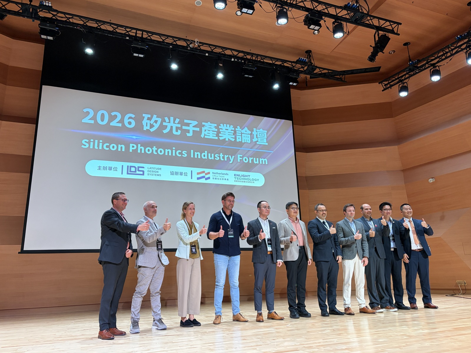
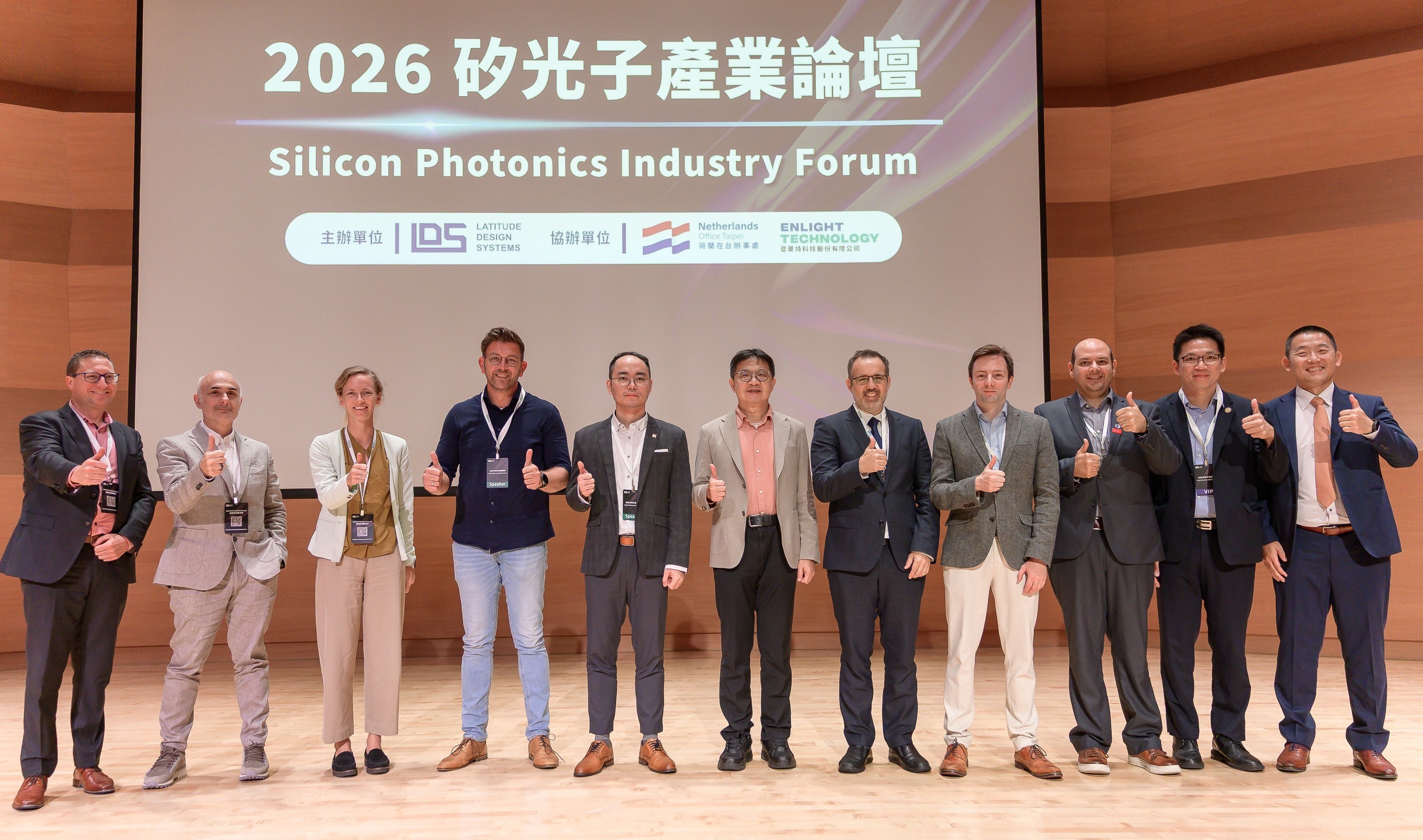
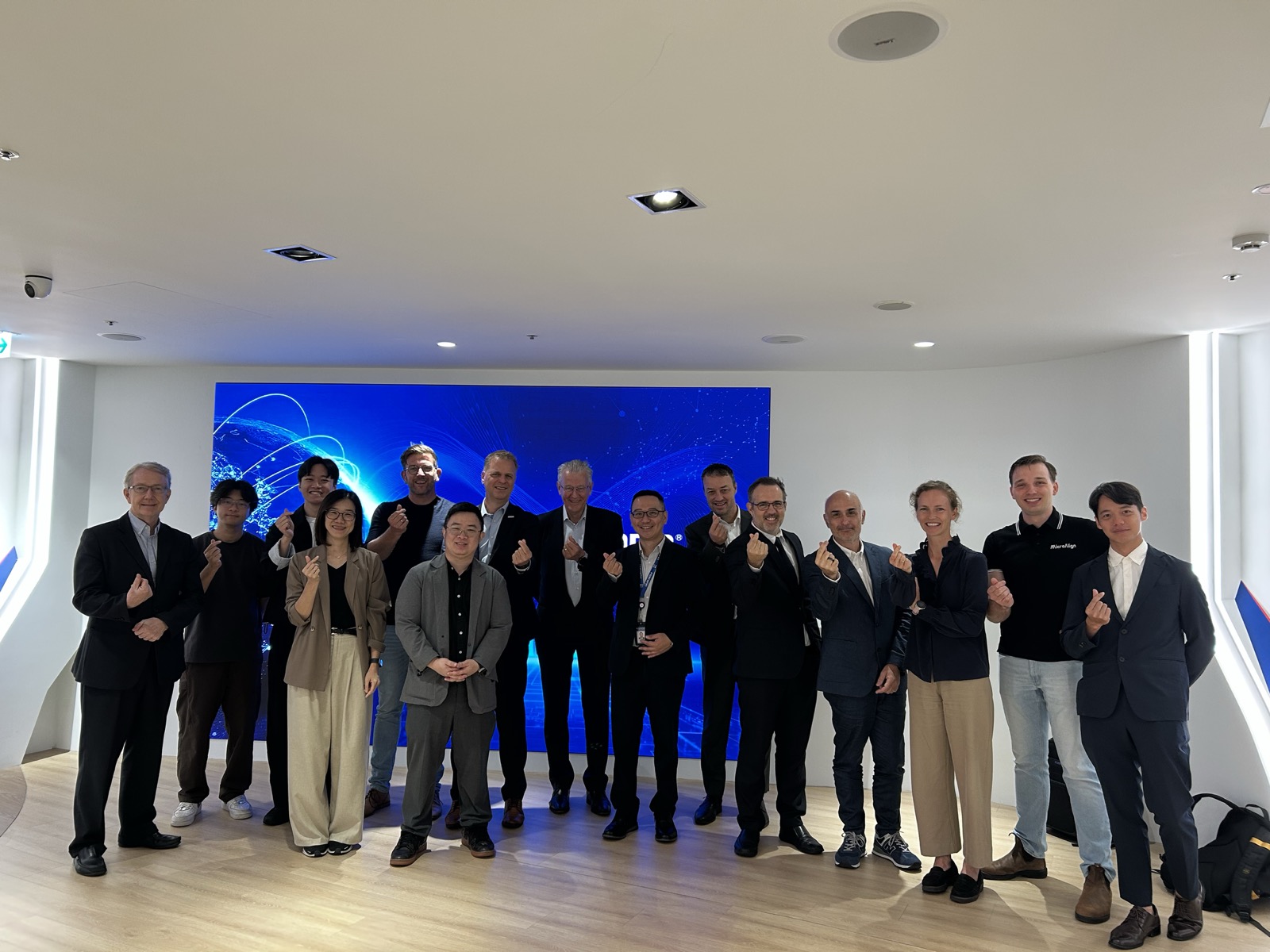
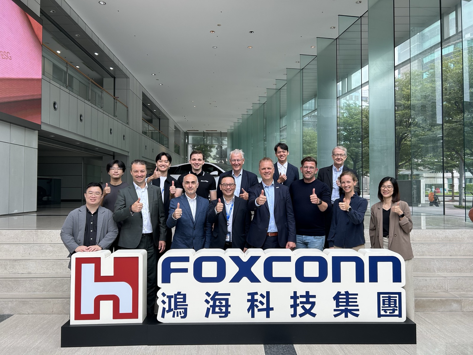
Taiwan is at the heart of the global semiconductor industry, and SEMICON offered a front-row view of the technologies, challenges and priorities shaping its next phase. The business program included a presentation at the Silicon Photonics Industry Forum organized by Latitude Design Systems, company visits to UMC in Hsinchu and HHRI/Foxconn and Wiwynn in Taipei, and a full day at the SEMICON exhibition.
SEMICON Taiwan brought together more than 1,300 exhibitors, with AI, high-performance computing, advanced packaging and system-level innovation among its main themes. That scale was impressive, and the conversations were even more valuable. I returned to the Netherlands with many new contacts and three observations that are particularly relevant to CoolSem Technologies.
1. Thermal management has become a roadmap issue
The first and most obvious takeaway was that thermal management is no longer a specialist topic discussed only by packaging or cooling experts. It is increasingly recognized as one of the factors determining whether the next generation of chips, optical devices and AI systems can deliver the required performance.
Companies across the value chain are investing in solutions ranging from advanced materials and packaging to cold plates and direct liquid cooling. During our visit, Wiwynn provided a particularly clear system-level perspective. Its latest AI infrastructure includes advanced liquid-cooling solutions designed for increasingly powerful accelerators and high-density racks. The company has even demonstrated cold-plate concepts intended to handle several kilowatts of thermal load. Wiwynn’s own technology roadmap shows how seriously the industry is taking this challenge.
My conclusion is that no single cooling technology will solve the entire problem. Better cooling at rack and package level remains essential, but we must also improve the thermal path from the heat sources in the semiconductors to the package. Once heat has accumulated inside the device, every subsequent cooling stage has a more difficult job. And this is exactly where CoolSem aims to contribute. Our technology is not an alternative to advanced package or system cooling. It is potentially an additional layer in the solution, addressing thermal resistance at wafer level.
2. The industry is moving from individual technologies to complete systems
My second takeaway is that innovation benefits from development across all levels of the semiconductor value chain.
This became particularly evident at the Silicon Photonics Industry Forum. The program connected materials, photonic platforms, lasers, packaging, thermal management, design tools and system integration. The underlying message was clear: silicon photonics may offer an answer to the bandwidth and energy-efficiency challenges of AI infrastructure, but commercial deployment requires all these elements to work together.
The forum attracted more than 300 participants and focused explicitly on moving optical interconnect technologies from R&D towards scalable manufacturing. As the event summary explains, this transition requires coordinated expertise across the entire chain, from materials and devices to packaging, cooling and systems.
We observed the same dynamic during our meetings with UMC, HHRI/Foxconn and Wiwynn. A foundry looks at process compatibility and manufacturability. A research institute explores the materials and device concepts needed for future applications. A system company starts with the performance, energy, reliability and cost requirements of an entire platform. All three perspectives are necessary.
For a company like CoolSem, this means we cannot validate our technology alone. We need device manufacturers, foundries, packaging partners and system companies around the table. The real opportunity is not simply to demonstrate lower thermal resistance, but to show what this improvement enables elsewhere in the system.
3. The application defines the optimal technology approach
The third takeaway may be the most important from a commercial perspective. Everyone understands that heat is a challenge. The real opportunity lies in identifying where advanced thermal management can make a meaningful and measurable difference and matching the right thermal approach to the specific device and application.
The most productive conversations quickly moved beyond the general need for improved thermal management and into the technical details: specific device structures, substrates, contacts, manufacturing temperatures and integration requirements. From there, we could explore what success would look like for each application, whether through lower junction temperatures, increased optical output, reduced wavelength drift, improved efficiency, delayed thermal roll-over or longer device lifetime. Moving forward, the most effective way to explore a potential cooperation is therefore to select a relevant device, define the desired performance improvement and validate it through a focused, measurable A/B feasibility study.
This is also consistent with the wider direction of the industry. UMC, for example, positions advanced packaging and heterogeneous integration as important enablers for higher bandwidth and power efficiency in AI applications, while also developing silicon-photonics capabilities for future data-center architectures. Its AI technology overview illustrates how process technology, packaging, power efficiency and connectivity are becoming increasingly interconnected.
In short - Turning conversations into experiments
As a conclusion, Taiwan left a strong impression. The semiconductor ecosystem is dense, pragmatic and highly interconnected. Companies are open to ambitious ideas, and quickly bring the conversation back to manufacturability, measurable value and a practical path to implementation. Thermal management is undeniably a hot topic, but recognition of the problem is only the beginning. The companies that succeed will be those that can demonstrate measurable value in a real device and ultimately across the wider system.
For CoolSem, the next step is to turn the connections made in Taiwan into focused technology discussions and joint experiments.
Finally, a sincere thank you to the Netherlands Office Taipei for opening doors and helping us access the impressive Taiwanese semiconductor ecosystem.
Additional coverage of the Event can be found in this article from SemiVision and the recap on YouTube.